Yes, display is there twice. Anyways, I’ve got this old dot matrix LCD, and for fun I decided to try to make a driver for it. It’s from a Brother LW-1 word processor which was a sort of electrical typewriter that included a printer and digital software for, well, word processing.
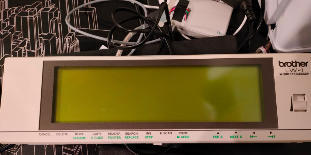
The display is a monochrome 640×128 pixel display that has a nostalgic potentiometer for adjusting the screen contrast. And yeah, it’s in an easy-to-access location for reason.
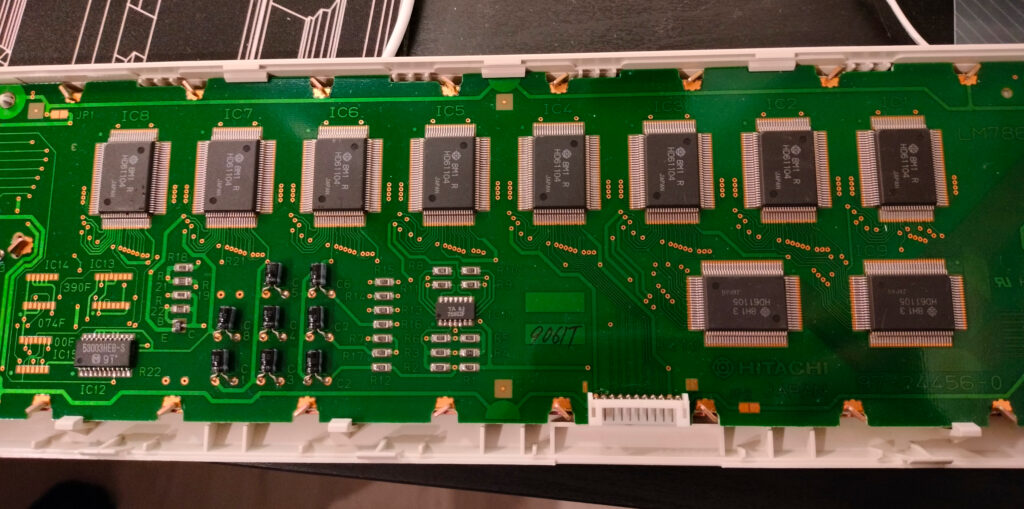
The display has a 11-pin connector, and opening the display case instantly reveals how it broadly speaking works. There are eight HD61104 column drivers and two HD61105 common drivers. There’s also a quad op-amp (TA75092) for buffering the four bias voltages and a Matsushita counter IC marked 53003HEB-S for which I couldn’t find a datasheet. On the other hand, luckily I could find one for HD61104 and HD61105, though even that datasheet is old enough that it has been scanned to a PDF. The datasheet did make the reverse engineering very easy.
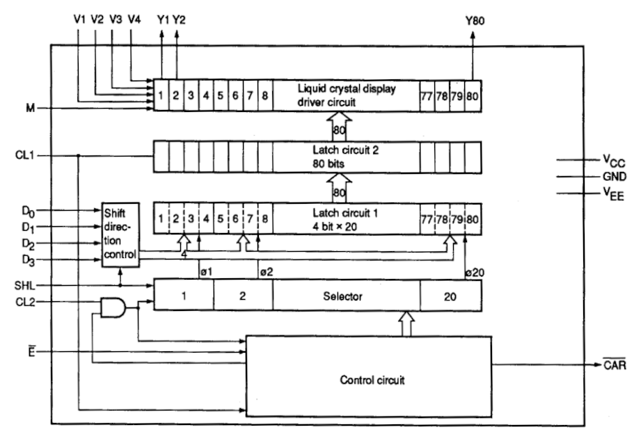
This block diagram from the HD61104 datasheet gives us an overview about how the chip works. M is a clock for the LCD driving signal, since the LCD requires that is driven with a AC signal that has zero DC component. CL1 is a row latching signal, and when it is driven low the new row data will be output. My oscilloscope tells me that the mystery counter IC 53003HEB seems to generate M from CL1 by dividing it by 40 as it outputs about 360Hz when CL1 is driven at about 14.4kHz.
The actual data is in the signals D0 .. D3 that is clocked by the falling edge triggered clock CL2. SHL selects the direction that the input bit are shifted in, and in this case it is connected to Vcc so that the first data bits will become the Y1..Y4 signals when the row is latched out.
Finally, the E is the usual enable pin and the CAR signal is used to cascade multiple HD61104s. The way that this works is that the CAR is pulled down after all eighty bits have been shifted in, enabling the next HD61104, and making it read the data.
The other part of the equation is the HD61105 which also has a block diagram.
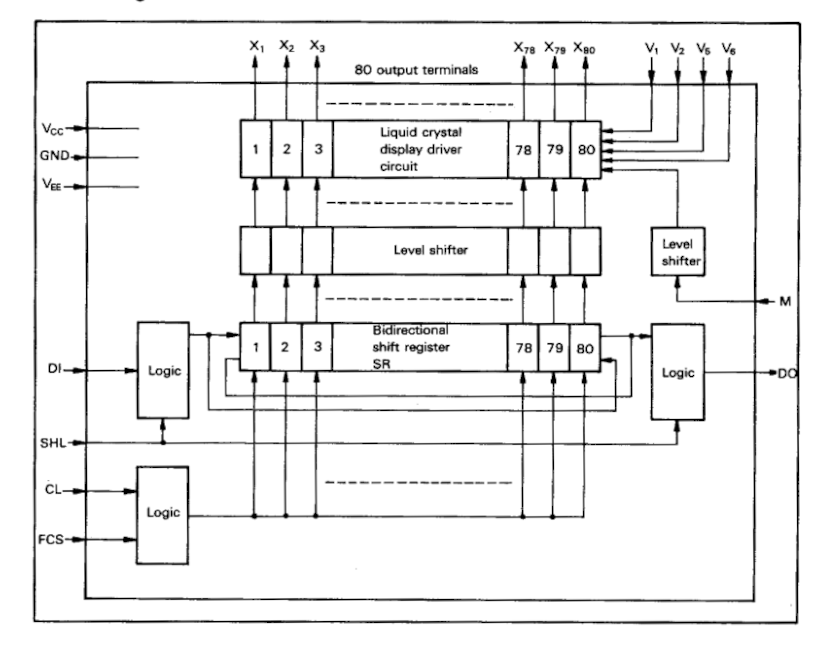
Similarly to the HD61104, we have the signals M, DI, SHL, DO, and CL. The data gets shifted in from DI and is clocked by CL, and after eighty clocks gets shifted out from DO. In addition there is a FCS pin that tells whether the clock triggers on falling or rising edge. Notice that there is no latching with this chip, and the shift register is directly connected to the output.
So the shift register of the HD61105s tells which rows are active and the latched outputs from HD61104s tells which pixels are turned on the rows. But we don’t want to have multiple active rows, so we put one bit 1 into HD61105 when we are drawing the first row, and then when we want to draw the next row we clock the HD61105 so that the next row is now active.
Since the datasheets tell the pinouts of the chips, it is a simple operation to find out the pins of the connector by a little poking with a multimeter.
The pins in the connector are:
VeeVccd0d1d2d3cl2cl1andcldignd(?)gndfor ICs
The datasheet specifies that Vcc should be about 5V. Vee is the negative voltage that is used to generate the bias voltages for the LCD with a resistor string that is then buffered by the op amp, and the voltage should be at minimum Vcc – 28V. In practice, this should be maybe about -20V since at -17V the contrast isn’t quite optimal even at the maximum level like a found out later.
Armed with this knowledge it is relatively simple to design a driver, at least in theory. But the fact that we need to output 4-bit data at 2 MHz to 3 MHz makes it a bit tricky since most microcontrollers aren’t really designed for it. Using an Attiny1606 I could do it by some bit trickery and careful examining of the resulting assembly, but it was far from optimal because Attiny1606 has limited memory and driving the display uses up almost all of the CPU time. In the end I was able to do run some animations from flash and have use UART to connect it to a computer. With some code I was able to interpret enough ANSI escape codes that I could run terminal applications like Vim on it. To do that in essence I duplicated my terminal using a nifty program named script to write the data also to my UART adapter in addition to terminal.
But I still didn’t find it quite satisfactory because of the limited memory. Attiny1606 has 1024 bytes of memory, and if we use 8×8 font we need (640*128)/(8*8)=1280 bytes of memory. Moreover, if we want to draw individual pixels, we need eight times as much memory i.e. 10240 bytes.
I tried to see whether I could use various SAM series microcontrollers but they are too slow to drive the display using CPU at 48MHz and they mostly didn’t seem to have DMA connected to PORT so it wasn’t possible either. Some of the had a parallel input capture so they could read multiple ports using DMA at the same time, but output was impossible.
Also at one point I was making a circuit using SAM S70, but there was a tiny little detail mentioned in the errata I hadn’t noticed.
The USBHS module does not function in 64-pin LQFP package devices.
SAMS 70 Errata page 34
Seriously Microchip?? No wonder I couldn’t get the USB module to work even after a couple days of debugging.
Anyway, the whole project was frozen for a time until I came across RP2040 and its nifty PIO (programmable IO) module. It seemed to be just what I needed. With it I should be able to drive the output without using much CPU. So I designed a PCB to for this application.
There was also the problem of how to generate the negative voltage. It could be done with a MC34063 in an inverting configuration (which I didn’t want to do because it’s MC34063). It could also be done with other voltage switching regulators with some trickery but would need careful examination if the chip isn’t designed for it. Also a voltage converter with discrete components (or combined with a microcontroller) is surely possible but in any case it will be somewhat complex because they need careful attention to many details. Also, an approach requiring a transformer would require a transformer which I would rather avoid if possible.
So I designed a simple discrete charge pump which doesn’t have feedback at all.
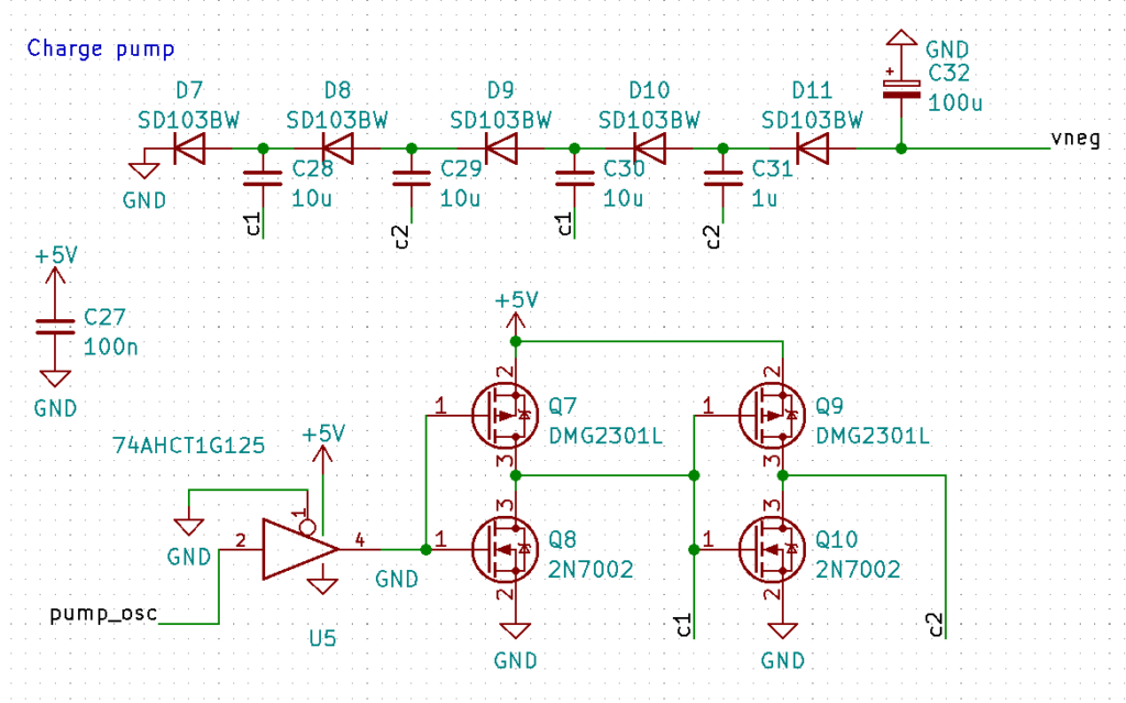
In this schematic the pump_osc is driver from the RP2040 using PWM, and the 74AHCT1G25 is a logic buffer that’s used as a 3.3V -> 5V level shifter since otherwise the P-MOSFETs wouldn’t really turn off. In the end I had to add a diode and a capacitor to get the voltage a bit higher, but luckily my PCB layout made adding them easy. All I had to do was to cut a trace, scrape off some solder mask and solder the two SMD components.
This approach worked pretty well, though it had its own shortcomings. It does require some space on the PCB (which I did have), and the output voltage isn’t very well regulated, especially when the input voltage from the USB cable can vary quite a bit. But it didn’t really present a problem because the display had a handy potentiometer to adjust the contrast. Also, this approach was very cheap!
With that problem solved the next thing was to see how well the PIO can be used to drive the screen. The conclusion was: very well. CPU didn’t need to care about the display at all! At least after it had set up PIO and DMA. It really doesn’t get much better than that.
It is very easy to use one SM (state machine) in one the two PIOs to drive D0..D3 and CL2. I had set up CL2 as a side-set pin and the data pins as regular out pins. Then just output the data using out and change CL2 and add some delays (or lower the clock speed) and that’s it.
But there’s still the problem how to drive CL1 and DI. Funnily enough I ended up with the same code for them both but the code runs in different state machines SM1 and SM2. So SM1 keeps track of how many half-bytes we have output in this row, and SM2 keeps track of which row we are currently in. I use the IRQ flags as a synchronization mechanism, so SM1 waits until SM0 sets the flag and SM2 waits until SM1 sets the flag. When SM0 outputs the data it sets the flag making SM1 decrease its internal counter by one, and likewise for SM1 and SM2.
Then the outputs are set to one in SM1 and SM2 for some time when the counter reaches zero, though I had to be a little careful so that SM1 only clocks its output when SM2 has set its DI output to 1. Also, there isn’t a nice way to set registers to values larger than 31. So what I did was that the CPU writes the maximum count into FIFOs of SM1 and SM2 at the startup, and the PIO code reads it and keeps the maximum value stored in one of the two registers.
In the end I had a working display driver even though the process wasn’t quite straightforward, I still wanted a way to use the driver. Naturally, I decided to use the USB peripheral of RP2040 as I’m already using an USB cable to power the device.
The TinyUSB library shipped also with Raspberry Pico SDK is pretty easy to use once you know how to use it but there isn’t much in the way of documentation. At least getting it to work was way faster than writing my own USB drivers (like I did for SAMD20) and debugging them, but the general knowledge of how USB works helped a lot when diving into TinyUSB source code to figure out how I should use it.
The USB reset interface was pretty handy even earlier in the development (when I was using Pico SDK USB stdio code) so I decided to use it when implementing my own USB code. It is pretty easy to do. Just add a custom interface driver (array of which should be returned from usbd_app_driver_get_cb), implement open and control_transfer_cb with the checks that the interface is correct and then call reset_usb_boot(0,0) in the right control request. Finally, add an interface descriptor without any endpoints to desc_configuration (and remember to update CONFIG_TOTAL_LEN).
Then a small Python program like
import usb.core
RESET_REQUEST_BOOTSEL = 1
CONTROL_OUT = 0
CONTROL_CLASS = 0x20
CONTROL_INTF = 0x1

ITF_NUM = 1
dev = usb.core.find(idVendor=0x0100, idProduct=0x0100)
dev.ctrl_transfer(CONTROL_OUT | CONTROL_CLASS | CONTROL_INTF,
                      RESET_REQUEST_BOOTSEL, 0, ITF_NUM, None, 1000)
can boot you into USB Boot mode so you can easily flash new code using Picotool.
I added a simple USB interface to write to the screen: an interface with one bulk output that writes data and one control request that sets the area that is drawn to.
So I just needed a program to write to the screen. I did code a framebuffer driver as a Linux kernel module (and yeah, it’s not very fun when kernel crashes and corrupts databases, like places.db that stores the history of Firefox.)
But it seems that there are not a lot of programs supporting fbs with 1 bit per pixel. Besides, updating the screen is easier with direct USB control as there’s apparently no way to use the kernel internal framebuffer API from outside the kernel. There is a nice helper for mmap based software framebuffer (in linux/drivers/video/fbdev/core/fb_defio.c) that keeps track of dirty pages but that isn’t very useful in this case as with 4K-sized pages we have only three pages.
However, there is one possible useful application for the framebuffer driver: using a framebuffer console. We can bind a /dev/fb1 to /dev/tty5 by running
con2fbmap 5 1that simply calls ioctl(fd, FBIOPUT_CON2FBMAP, &map). Now we can use
chvt 5to make /dev/tty5 the foreground terminal, and we can use it as a display for a computer. It isn’t very useful for me right now, but it could be used as a simple display with for example Raspberry Pi.
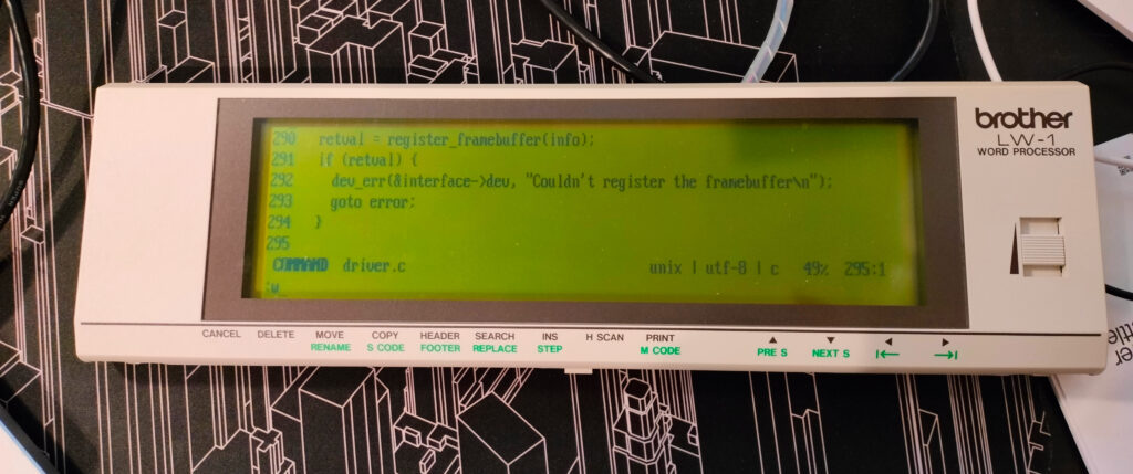
In the end I wanted to try out using LVGL as it supports monochrome displays and I could write easily different renderers, one for the display and one for SDL2 for development. Sure, I could just write code that writes individual pixels but LVGL has inbuilt fonts and other nice things.
Now I just have to decide what I want to show on the display and write the code for it.